HBF and zHBM, Explained: Samsung and SK Hynix Give Opposite Answers to the Same Memory Problem
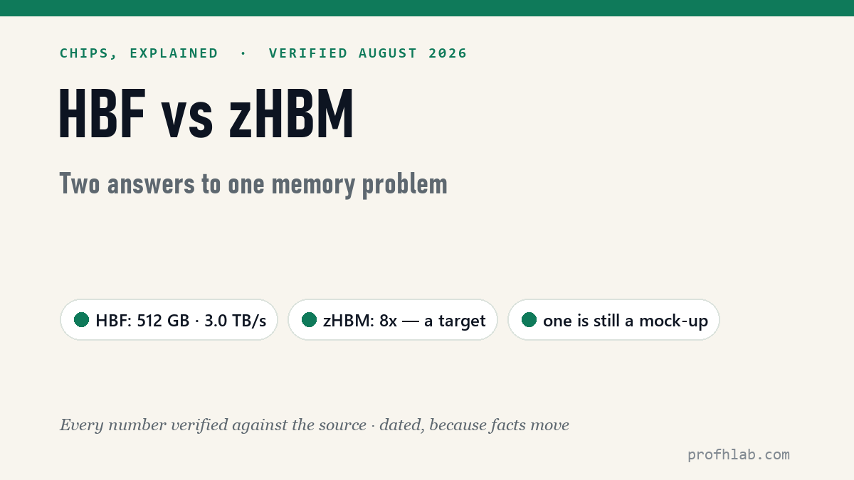
On August 4, 2026, in Santa Clara, Samsung Electronics and SK Hynix stood up at the same trade show, named the same problem — and gave exactly opposite answers. SK Hynix stretched NAND flash sideways to buy capacity (HBF: up to 512 GB per stack, up to 3.0 TB/s).
Samsung stacked DRAM straight on top of the accelerator to shorten the distance (zHBM: an 8x performance target against HBM5). And the finish line of this race is not a data center. It is the robots that are supposed to be walking semiconductor factory floors in 2030. Figures verified August 6, 2026.
Same show, opposite answers
The setting was the opening day of FMS 2026 — the memory and storage industry’s biggest annual event, in its 20th year, at the Santa Clara Convention Center. Two companies opened their presentations with nearly the same sentence: compute is getting faster at a furious rate, and memory cannot keep up.
Kim Chun-sung, who heads solution development at SK Hynix, framed it this way: in the agentic-AI era, token throughput is growing at an unprecedented pace, while DRAM bandwidth is failing to keep up with the advance of compute performance.
The diagnosis was identical. The prescriptions pointed in opposite directions. SK Hynix chose to go sideways. Samsung chose to go up. And the two roads run much farther than the search phrase “what is HBF” suggests — all the way to robots.
HBF, explained: stack NAND, buy room to remember
HBF stands for High Bandwidth Flash. The one-letter difference from HBM (High Bandwidth Memory) is no accident: where HBM stacks DRAM to buy speed, HBF stacks NAND flash to buy capacity.
The first standard specification, published on August 4 by SK Hynix and SanDisk, reads like this: based on 8- and 16-die NAND stacks, up to 512 GB per stack, with bandwidth split into three grades (Grade 1–3) spanning roughly 0.4 TB/s to 3.0 TB/s. For the interconnect they chose UCIe, an open standard rather than any vendor’s proprietary link, so the stack can attach to GPUs, CPUs, and other processors. The standard document covers not just electrical characteristics but die-stack process reliability, packaging guidance, and software guidelines for data I/O.
The key question is: why NAND? Look at the data AI inference actually handles, and the data that gets read over and over dwarfs the data that must be freshly computed each moment — model weights, the KV cache that balloons as a conversation gets longer, the document piles that RAG keeps consulting. Keeping all of that in expensive DRAM is wasteful; parking it on an SSD is too slow. HBF is a new tier that slots in between: not as fast as HBM, but fast enough — and far cheaper and larger than DRAM can be.
At the same event, SK Hynix also showed for the first time the wafers and parts of its 10th-generation V10 375-layer 4D NAND, claiming 2.5x performance per watt over the previous generation, with high-capacity enterprise SSD production on that base slated to begin early next year. A new tier, and the NAND to fill it, on one stage.
zHBM, explained: Samsung went up instead
Samsung’s card points the other way. The z in zHBM is the z-axis — height. Until now, HBM has sat next to the AI accelerator on an interposer. zHBM puts the memory directly on top of the accelerator, vertically.
The idea is simple: when data travels a shorter distance, it moves faster, runs cooler, and burns less power. Samsung’s stated targets against HBM5: up to 8x per-GPU performance, up to 3x performance per watt, and more than half the thermal resistance removed. Between accelerator and memory sits a custom “interlayer” that lets memory capacity and compute functions be tuned to a customer’s AI processor.
Here is the part to be cold-eyed about. What Kim Kyung-ryun, a vice president in Samsung’s DRAM development organization, put on stage is a mock-up, not a production part — closer to a declaration of direction. The 8x figure is a target, not a measurement. If a headline left you thinking “Samsung built memory that is eight times faster,” that is not what happened.
On the NAND side, Samsung brought real hardware too: V10 BV-NAND stacked past 400 layers, using wafer bonding and a triple-deck cell connection to fit about 58% more data into the same footprint than the prior generation. And zNAND-O — V-NAND combined with through-silicon vias (TSV), packaged in 4- and 8-die stacks — aims at on-device AI: how fast a phone or PC can load a model.
HBM4 vs HBF vs zHBM: one table, seven criteria
Read each company’s press release on its own and both sound magnificent. So here they are on one table — the frame the news stories don’t give you, with only the criteria that matter for judgment.
| Criterion | HBM4 (today’s workhorse) | HBF (SK Hynix · SanDisk) | zHBM (Samsung) |
|---|---|---|---|
| Base device | DRAM | NAND flash | DRAM |
| Where it sits | Beside the accelerator, on an interposer | Beside the accelerator — a new tier between HBM and SSD | Directly on top of the accelerator (vertical) |
| Disclosure level | In production and shipping | Standard specification published | Mock-up (structural proposal) |
| Headline numbers | Per generation standard | Up to 512 GB · 0.4–3.0 TB/s | 8x performance, 3x perf/W vs HBM5 (targets) |
| Interface | JEDEC standard | UCIe (open) | Custom interlayer |
| Data it targets | Live computation data | Repeat-read data: weights, KV cache, RAG | High-speed data hugging the compute |
| Maturity | Commercial | Standardization begun | Concept-validation stage |
Laid out this way, the three are not rivals so much as layers with different jobs. HBM4 is earning money today. HBF is an attempt to lay one more tier underneath it. zHBM proposes changing the direction of stacking altogether. Any summary of the form “HBF replaces HBM” only works if you delete the maturity row.
The investor read: three things to keep straight
Search interest in “HBF stocks” is a natural reflex — but between a published standard and actual production-and-supply contracts there usually sit several years. The 3D DRAM concept SK Hynix showed the same day (DRAM stacked on a GPU, putting larger-than-SRAM capacity next to the compute) likewise has no commercialization schedule. What can be verified today ends at “who picked which direction.” Three cautions, stated plainly:
- zHBM is a mock-up. What was shown is a structural demonstrator; production timing and absolute bandwidth numbers are unpublished, and “8x vs HBM5” is a target.
- HBF has no price and no named customers yet. The standard exists; adoption, unit economics, and production schedules do not. Whether the tier opens is the market’s call.
- Watch the theme-trade heat. With both of the above unsettled, the risk of a theme getting priced ahead of the facts is real. This article recommends no security, in either direction.
Why this story ends on a factory floor
So far this sounds like a data-center story. Overlay the plans both companies have already published, and the picture changes.
At NVIDIA GTC 2026 in March, SK Hynix vice president Do Seung-yong said the company will build an autonomous fab by 2030, on three axes: an “operation AI” as the factory’s brain, “physical AI” as its body, and a digital twin for simulation. Vision-based robots and AMRs already handle parts supply, chemical handling, and equipment maintenance — with results the company quantifies as over 50% faster equipment-maintenance and defect-analysis handling, and roughly 30% lower parts inventory.
Samsung, on March 1, announced it will convert its factories at home and abroad into “AI autonomous factories” by 2030 — phase one: digital-twin simulation of the entire flow from inbound materials to shipment, plus AI agents for quality, production, and logistics; phase two: AI across environmental safety; phase three: humanoid manufacturing robots — operating bots, logistics bots, assembly bots, safety bots. Executive vice president Lee Young-soo framed the goal as moving past simple automation to production sites where the AI understands the floor and executes the best decision on its own.
See the connecting line? A robot making its own calls on a factory floor has no time to ask the cloud. It must carry model weights in its body, pile what it just saw into a cache, and read it back in milliseconds. That is precisely the data HBF is aimed at. A tier being built today for data-center racks sliding, a few years later, onto a robot’s back is not a stretch — it is the straight-line extension of both companies’ own announcements.
To be fair: nobody has written “robot HBF” into an official roadmap yet. But stretch the arrows the two companies drew on August 4, and they point out of the data center.
How to read announcements like these
First, always separate announcement stages. From a single event: HBF is a “standard published,” zHBM is a “mock-up shown,” and V10 NAND is “production starting early next year” — three different maturities. The headline numbers — 8x, 3.0 TB/s, 58% — are, respectively, a target, a spec ceiling, and a density gain. Put them on one scale and you will reach a wrong conclusion every time.
Second, the winnings accrue to the layer, not to one company. HBF adopting the open UCIe standard means the tier could open into a market not captive to any single GPU vendor — NAND supply, packaging, controllers, and interconnect IP all move with it. zHBM, stacking directly on the accelerator, makes foundry-and-packaging capability and custom co-design the battleground. The two roads demand different muscles.
Will HBF replace HBM, and can anyone buy zHBM yet?
Q. Is HBF going to replace HBM?
No — they do different jobs. HBM feeds live computation; HBF is a proposed cheaper, larger tier between HBM and SSDs for repeat-read data like model weights and KV cache. The honest comparison keeps the maturity column: HBM4 ships today, while HBF has just published its first standard.
Q. Is zHBM something you can buy?
No. What Samsung showed at FMS 2026 is a mock-up demonstrating a structure, with target numbers. No production timing or measured bandwidth has been published.
Q. What actually exists today, then?
A published HBF standard (up to 512 GB, 0.4–3.0 TB/s, UCIe), real NAND hardware shown by both companies (SK Hynix’s 375-layer V10; Samsung’s 400+ layer BV-NAND), and stated 2030 factory plans. Prices, customers, and production dates for the new tiers: none yet.
Two speeds
Technology always runs at two speeds. The memory tier is sprinting — a standard in August, production NAND early next year. The robots meant to someday carry that tier are still on 2030 roadmaps. Watch where the two speeds meet: it will be a factory floor.
This article is informational only. Figures, schedules, and specifications are as verified on August 6, 2026 and can change; nothing here is investment advice.
Part of the Physical AI library — research decoded and machines compared, in plain English: profhlab.com/physical-ai.
A primer on how HBM works and why the memory wall matters
Full index
Every guide in the Physical AI library — 27 of them, grouped so you can find the one you need.
Start here
- Physical AI Foundations: World Models, Robot Foundation Models, and Sim2Real — From Zero
- Physical AI Explained: Why a Chatbot Knows the Cup Falls but a Robot Doesn’t
- The Physical AI Toolbox: Six Free Simulators, a $249 Hardware Ladder, and What the 2026 Papers Admit
Research papers, decoded
- RoboVLMs, Explained: What Actually Makes a Robot Foundation Model Work
- Ψ0 (Psi-Zero), Explained: The Humanoid Foundation Model That Learns From Human Video
- MotionWAM, Explained: One-Shot Imagination Brings Real-Time Humanoid Loco-Manipulation
- XHugWBC, Explained: One Policy That Drives 12 Different Humanoids
- Vision-Tactile Pretraining, Explained: A Robot Hand Learns Human-Like Dexterity From a Webcam
- TouchWorld, Explained: A Robot Hand That Predicts Touch Before Making Contact
- HOUND and APT-RL, Explained: One Transformer Brain for Walking, Running, and Jumping in the Wild
Machines, priced
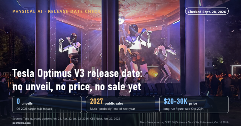
- Tesla Optimus V3 Release Date, Price and Specs: What Tesla Has Confirmed
- Buying a Humanoid Robot in 2026: What a Unitree R1 Really Costs, Retail vs Import
- Robot Dog Prices in 2026: From ≈$2,900 to ≈$71,000 — and Spot Still Has No Price Tag
- Tesla FSD Goes Subscription-Only in Korea — and the ‘5-Year Break-Even’ Everyone Quotes Is Wrong
Home robots, tested
- Narwal Freo Z10 Ultra Review: 18,000Pa, a 75°C Mop Wash, and Three Honest Drawbacks
- 22,000Pa vs 240 Air Watts: Robot Vacuum Suction Numbers, Decoded (2026)
- Robot Vacuum or Stick Vacuum? I Split Housework Into 10 Tasks — Only One Truly Overlaps
- The Sour Smell Isn’t the Mop: Robot Vacuum Odor by Zone, and a 7–9x Consumables Gap
- Drain Height Decides Your Robot Vacuum: Samsung 0.4 m, Roborock 50 cm, LG 1.5 m
- Robot Vacuum Repair Costs 2026: A $140 Fix and a 56.5% Resolution Rate
- Robot Vacuum Subscription vs Buying: What iRobot Select Really Costs
- Are Window-Cleaning Robots Worth It? The Break-Even vs Hiring a Pro
- Smart Speakers in 2026: The Hardware Is $99 — the Assistant Is the Real Price
- Serving Robot Costs in 2026: $399 a Month, and Why 73.3% Saw No Change
Chips & companies
- ▸ HBF and zHBM, Explained: Samsung and SK Hynix Give Opposite Answers to the Same Memory Problem (you are here)
- Korea’s Chip Equipment Makers, Compared: Profits Fell 68% — So Why Did Pay Jump 29%?
- Samsung DS vs DX: One Company, a $450,000 Bonus Gap — and Why the Simple Story Is Wrong
- ASML Korea’s Starting Pay Is $31K — or $46K: Anatomy of a 2.15x Salary-Data Gap
Looking for the other library? Generative AI — tools, tested →
Prof.’s H Newsletter
One short email a month, with the numbers in it
What actually moved in AI hiring, AI prices, and the scams aimed at older Americans. Counted here, dated, and linked to the source. One email a month, and your address goes nowhere else.